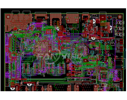
One-stop service
Experienced Team
Effective communication is the key to success for the projects.
We appreciate files and main cases through email and details on Skype.
Please sign in and contact our staff to talk projects, thanks.The files we need for PCB design & layout
Effective communication is the key to success for the projects.
We appreciate files and main cases through email and details on Skype.
Please sign in and contact our staff to talk projects, thanks.The software we use
Effective communication is the key to success for the projects.
We appreciate files and main cases through email and details on Skype.
Please sign in and contact our staff to talk projects, thanks.Our design basis
Effective communication is the key to success for the projects.
We appreciate files and main cases through email and details on Skype.
Please sign in and contact our staff to talk projects, thanks.The files we can send to you
Effective communication is the key to success for the projects.
We appreciate files and main cases through email and details on Skype.
Please sign in and contact our staff to talk projects, thanks.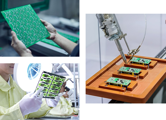
Design Process
PCB design + PCB fabrication + SMT placement +
stencil fabrication + BOM matching
One-stop service
| Maximum number of layers | 42 layers |
| Maximum PIN count | 110,000+ |
| Min BGA PIN pitch | 0.3mm |
| Highest speed signal | 60GHZ |
| Min. line width | 2.4mil |
| Max. number of connections | 78000+ |
| Max. number of BGA-PINs | 2912 |
| Min. line spacing | 2.4mil |
| Maximum number of layers-tset1 | 42 layers |
| Maximum PIN count | 110,000+ |
| Min BGA PIN pitch | 0.3mm |
| Highest speed signal | 60GHZ |
| Min. line width | 2.4mil |
| Max. number of connections | 78000+ |
| Max. number of BGA-PINs | 2912 |
| Min. line spacing | 2.4mil |

